
My friend saved money for two years to buy the graphics card he had been dreaming about. The day it arrived he texted me a photo of the box like it was a newborn. An hour later he texted again: his room had turned into an oven, the fans sounded like a hairdryer stuck on high, and his electricity meter was, in his words, spinning like it owed someone money. He was thrilled and a little shaken at the same time.
That tiny, overheating room inspired me to write this whole series of 3 articles on the physical cost of AI what it actually costs the planet to answer your query. The heat, the power draw, the bill you never see coming, all of it is baked into the chip long before it answers a single question. So let us start where the chip does, with a fistful of sand.
What's inside
The quartz that becomes an AI brain is dug out of the ground in places like Spruce Pine, North Carolina, a town of about 2,000 people that happens to sit on some of the purest silica on Earth. From there it is melted, purified, sliced, and printed on by machines that cost more than a passenger jet. By the time that sliver of sand becomes one NVIDIA Blackwell chip, it has soaked up more electricity and more clean water than most people would guess. And it has not answered a single question yet.
We picture AI as something that lives "in the cloud." It does not. It lives on a chip, and the chip is a small, thirsty, white-hot city.
1. First, what is actually on that chip? Three very different residents.
When people say "AI chip," they are really pointing at a package that holds three kinds of silicon doing three different jobs. The easiest way to picture it is a city.
Logic (the GPU compute die) is the workforce. This is the part that does the actual thinking, the math behind every word AI generates. NVIDIA's Blackwell logic die packs about 208 billion transistors (NVIDIA, 2024). A transistor is just a microscopic on/off switch, so picture 208 billion light switches flipping billions of times a second on a chip the size of a stamp. That frantic switching is where most of the heat and power come from.

A 300mm silicon wafer, the canvas every AI chip is printed on. Photo: Peellden (CC BY-SA 3.0).
Memory (the HBM stacks) is the warehouse district. The workers are useless if the materials are far away, so AI chips glue the memory right next to the logic. This is High Bandwidth Memory, or HBM. Instead of spreading memory chips flat like a parking lot, engineers stack them into towers, like a parking garage going vertical to fit more cars on the same land. SK Hynix's current stacks are twelve DRAM layers tall, 36GB each (Tom's Hardware, 2025), and a single Blackwell chip carries up to 192GB of it (NVIDIA). Memory does not switch as violently as logic, so it burns less power, but it runs hot because it is packed so tightly.
I/O (the input and output dies) is the roads and ports. These move data on and off the chip and between chips. Without them the city starves. They are the least glamorous and, luckily, the least power-hungry part.
A modern AI chip is not one chip. It is a city of workers, warehouses, and roads, each built in a different factory, in a different country, then fused onto one board.
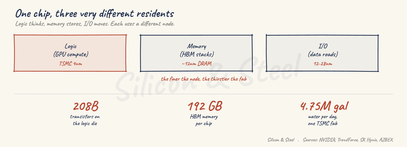
Logic, memory and I/O each live on a different node and carry a very different power and water bill.
2. Now the part everyone hears, and nobody explains: "nanometers."
You will see chips described as "4nm" or "3nm" or "2nm." Think of the number as how fine the pen is that draws the circuit. A finer pen draws smaller, more tightly packed transistors, so you fit more thinking into the same space and waste less energy per calculation. Smaller number, finer pen.
One honest caveat: these ‘nm’ numbers stopped being literal measurements years ago. "4nm" does not mean anything on the chip is 4 nanometers wide. It is now more of a brand name for a generation of technology. But the rule of thumb still holds: lower number, newer, denser, more expensive, and far harder to make.
Here is the key point, because not every resident of the chip uses the same pen:
The logic (GPU) uses the finest pen there is. Blackwell is built on TSMC's 4NP process, a roughly 5nm-class, leading-edge node (TrendForce, 2024). This is the node we are really talking about when we talk about the AI boom. It is the most power-hungry and water-hungry silicon on Earth to produce, because it needs the EUV lithography machines, the ones that draw about a megawatt each while running, roughly what 750 homes pull at once.
The memory (HBM) uses a slightly coarser pen, an older DRAM node around the 10-to-14nm class. Still advanced, but not the bleeding edge.
The I/O and power chips use much coarser pens, often 12nm to 28nm or older, made in cheaper, less thirsty fabs. Mostly used in Automotive applications.
So when a headline says "the world is fighting over 3nm and 2nm capacity," it is fighting over the logic. That is the choke point. That is where the power and water bills spike.
3. The Interesting Numbers
Here is the number that tells you where AI really sits in the physical world: TSMC, which makes almost all the leading-edge AI logic, used close to 25,000 gigawatt-hours of energy in 2023 and consumes around 9% of all the electricity on the island of Taiwan (Statista; New Lines Institute, 2025).
